Difference between revisions of "Materials Processing and Fabrication"
| Line 20: | Line 20: | ||
=== Self Assembly === | === Self Assembly === | ||
[[Self Assembled Materials]] | Current research into [[Self Assembled Materials]] is pointing to ways that thin layers can be built up in a highly organized manner. This provides more control of the dipole moment of applied surfaces. | ||
==Poling== | ==Poling== | ||
Revision as of 14:45, 21 September 2009
| Previous Topic | Return to Organic Photonics Applications Menu |
A great amount of research effort is devoted to developing new ways to apply materials to substrates in extremely thin organized layers so as to improve performance and to make the large scale manufacturing of devices economical. Some techniques that are practical for developing a single device with record breaking efficiency would not work for making millions of devices in a production line. Also engineers must be concerned with the durability of devices under real world conditions of heat, moisture and oxygen. At the same time new nanotechniques and self assembly make it possible to build novel structures virtually one molecule at a time.
See Wikipedia Microelectromechanical systems
Deposition
Spin Coating
see Wikipedia Spin Coating
Crystal growth
Layer by layer deposition
Self Assembly
Current research into Self Assembled Materials is pointing to ways that thin layers can be built up in a highly organized manner. This provides more control of the dipole moment of applied surfaces.
Poling
Optically assisted poling
Electric Field poling
Patterning
Nanoimprinting
Soft Lithography
Thermomechanical nanolithography
Etching
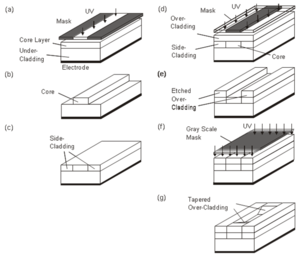
Polymer waveguide fab: RIE
Reactive Ion Etching (RIE) is used to convert a slab waveguide into a channel waveguide.
- First a slab is prepared with a core layer (higher index of refraction) is placed on a polymer undercladding on a silicon substrate.
- A metallic photo mask is applied to protect the core material.
- A plasma of oxygen is used to eat away the unmasked portion of the polymer.
- The metalic mask is removed and the ribbon of core material is fully encased with overcladding.
Sol-gel waveguide fabrication
This technique builds a complex sol-gel waveguide using completely wet techniques (no vacuum required). Direct illumination by UV through a mask is able to fix portions of the core in place, while unfixed portions are washed away. A series of steps like this can be used to build a complex device.
Polymer waveguide fab: Results
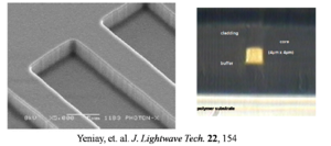
The company Photon X has commercialized the polymer waveguide process. The SEM (5micron line shown) shows very smooth sidewalls from a high quality etching process. Walls can only have roughness of 40-50 nm before there is significant optical loss. The polymer waveguide shows excellent light transmission through a 4 mum x 4 mum waveguide core that has been designed to couple very well with an optical fiber.
See Yeniay [1]
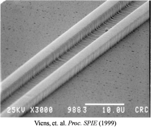
Polymer waveguide fab UV curing
This waveguide is created using the same UV curing process that is used with sol-gels. This shows two waveguides very close to each other. The channel is very difficult to control using photo etching process. The SEM shows a little cross striation but overall very good quality results.
See Viens 1999 [2]
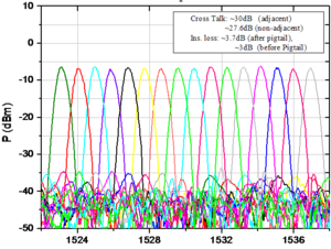
Polymer athermal Array Waveguide Gradiant AWG filter
An array waveguide gradiant is used to separate out wavelengths into separate ports. To characterize the device you shine a variety of wavelengths through the device simulating various information carriers and then measure the output from each port. The fluorinated polymer device was able to achieve these results:
- Insertion loss: 3 dB
- Adjacent crosstalk: -30dB
- Non-adjacent crosstalk: -28 dB
This passive polymer technology is being used to connect servers (interconnects) in server forms over very short distances with tremendous data rates.
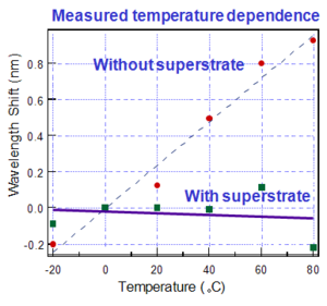
An athermal device performs equally well at different temperatures without temperature control.
Wavelength Temperature Dependence dλ/dt :
- without superstrate: 12pm/ °C
- with superstrate: - 0.5pm/ °C
See Gao 2002 [3]
References
| Previous Topic | Return to Organic Photonics Applications Menu |

