Electro-optic Polymers and Devices
| Previous Topic | Return to Organic Photonics Applications Menu | Next Topic |
Electro optical materials change their index of refraction when an electric field is applied. This effect can be used to create devices such as optical modulators and switches.
Electro-optic Polymer Materials and Devices
Electro – optic polymers compared with conventional materials
The Pockels coefficient measures the picometers of displacement of the wavelength per volt of applied field. the Electro-optic or Pockels effect
- <math>\Delta n= \frac {n^3 r E} {2}\,\!</math>
where
- <math>n\,\!</math> is the refractive index
- <math>r\,\!</math> is the Pockels coefficient
- <math>E\,\!</math> is the applied electric field
The existing technology uses lithium niobate LiNb03. Modulators made from this material are made from single crystals that are etched, diffused with Ti and then applied with electrodes in a multistep process.
Polymer waveguides can be manufactured with simpler photo patterning processes using bulk applied materials.
| LiNbO3 | EO Polymers | |
|---|---|---|
| Pockels coefficient | 30 pm/V | 170-370 pm?V |
| Drive Voltage | 4 V | 0.5 V |
| Index dispersion (nm -n0) | 3.1 | 0.1- 0.2 |
| Operating Speed | 20-40GHz | 110 GHz |
| Insertion Loss | 4 dB | 8 dB |
| Waveguide Fabrication | Ti diffusion | Direct Photo Patterning |
EO polymers have 6 to 10 times as much effect as LiNbO3. This means they can operate with much smaller drive voltages (.5 V) thus making them quite practical.
The index dispersion is the difference between the speed of the microwave and the optical field. To be efficient these waves should travel at the same speed. If the difference is great as in Li Nb03 different the waves can’t travel far before they have to be resynchronized. EO materials have far lower index dispersion.
The operating speed of LiNb03 of 20-40 GHz is still compatible with current computing requirements. In the future 110 GHz that is possible with EO Polymers will be needed.
The main problem of EO polymers is the loss which makes them suitable for short distance. Techniques that were used to decrease the loss with passive polymers may be used to solve this problem with active EO polymers.
Desirable modulator characteristics
These are the characteristics we are seeking in an organic modulator.
- Loss: 6-8dB fiber-to-fiber - this is also known as insertion loss.
- Vp ~ 0.3 - 1.0V
- Bandwidth: > 20GHz
- Operating Temperature < 70°C
- Optical Power Handling > 50mW
- Wavelength: 1550nm
There are two figures of merit (FOM) that represent a goal one for the device and one for the material
Modulator Device Figure-of-Merit
Device FOM = (Insertion loss in dB) <math>*V\pi\,\!</math>
Modulator Material Figure-of-Merit
Material FOM = :<math> n^3r_{33} / \alpha\,\!</math>
Where
- <math>n^3\,\!</math> is the index of refraction cubed
- <math>r_{33}\,\!</math> is the eo or pockels coefficient.
\alpha = material loss in dB/cm
Hybrid polymer/sol-gel technology
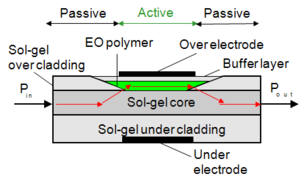
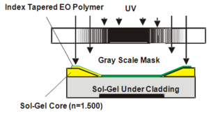
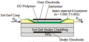
This is a novel device structure developed at UW and UA. By physically tapering the cladding (using gray field lithography) it is possible to pull the light from the sol-gel core into the active EO polymer which has a significantly higher refractive index than the sol-gel cladding. This gives a robust connection to the optical fiber on either side while protecting the EO polymer. This addresses some of the problems with EO polymers. The very low driving voltage of .65V and 170pmV EO coefficient in the device is a significant improvement.
Using advanced EO polymers
- Unique device design allows > 100% poling efficiency
- Record high EO coefficient r33 of 170pm/V demonstrated:
- Vp MZ Modulator 0.65 V: recently published in APL, Enamii, et. al.,
Hybrid EO-polymer/sol-gel waveguide modulators benefits
Basic premise: A robust waveguide device can be constructed using photosensitive hybrid sol-gel. Different functions can be implemented by overlaying an active film. The wave can be brought to the film and then returned to the sol-gel waveguide.
Advantages
- Low fiber-waveguide coupling loss- Waveguides can be matched to optical fibers for low coupling losses
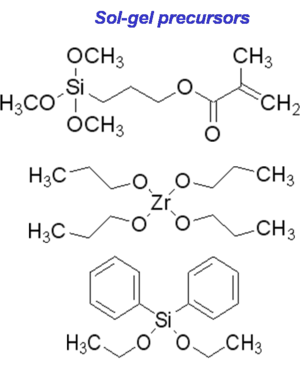
- Hybrid sol-gels allow good control of refractive index and dimensions
- Low waveguide propagation loss
- All wet etching process in isopropyl alcohol reduces fabrication difficulty and expense.
- Efficient poling
- Photostable material at fiber/wg interface- Sensitivity to functional material degradation is low.
- Increased ease of packaging
- Photosensitivity allows development of fine optical features.
- Adiabatic transitions can bring the wave up to an overlay film and back.
- Functionality can be added by overlay of active materials such as
- EO polymers
- chemical or biological agent sensitive media
- Devices can be easily “upgraded” with better functional materials.
Optimizing Vπ- some issues
How do we make the drive voltage lower? The equation tells us how.
- <math>V_\pi = \frac {\lambda d} {n_{dev}^3 r^{dev}_{ij} L \Gamma}\,\!</math>
where
- <math>d\,\!</math> = electrode separation
- <math>n_{dev}\,\!</math> = refractive index
- <math>r_{ij}^{dev}\,\!</math> = EO coefficient
- <math>L\,\!</math> = active length
- <math>\Gamma\,\!</math>= optical/electrical overlap
There are several variables here that could be modified to lower the drive voltage. You can’t usually change the wavelength since that is dictated by the telecom system. You can reduce the separation on the electrodes because the EO effect cares about field not voltage. You could also increase the index of refraction, increase the EO coefficient, increase the length or in increase the optical /electrical overlap gamma. However:
- Large r33 is often accompanied by lowering of the first excited state energy leading to increased absorption this limits making the device longer.
- Device designs focused on achieving low Vπ often sacrifice efficient fiber-to-waveguide coupling or employ long waveguides
- Achieving large r33 in a waveguide device places significant constraints on the cladding materials
- Efficient poling often leads to increased loss.
Importance of the buffer layer
Development of organics with large r33 coefficients is only the first step in making useful modulators.
Buffer layers are needed for waveguiding purposes and keeping the polymer away from the electrodes to reduce losses.
Buffer layers should have low resistivities, high transmission, and tunable refractive indices.
Sol-gels are attractive materials as buffer layers.
Poling Polymers Basics
<swf width="300" height="200">http://depts.washington.edu/cmditr/media/electropolar.swf</swf>
Before poling the chromophores with a permanent dipole moment are randomly oriented. After heating to a temperature near the Tg and applying an electric field the chromophores become aligned. To first order the degree of alignment is directly proportional to the applied electric field. In reality we only get about 20% alignment (not as good as the illustration).
See also Second-order_Processes#Poled_Polymers
Standard guest host EO polymer
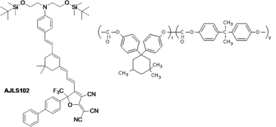
Amorphous Polycarbonate and polymethyacrylate are standard EO materials.
AJLS102 developed by Alex Jen at UW. It has a donor (the N end), an acceptor (the tri cyano end) and a conjugated bridge which produces a strong dipole that that the field can be oriented. This arrangement is critical for EO activity.
See Enami, et. al., APL 89, 143506 (2006)
EO polymers with very high r33
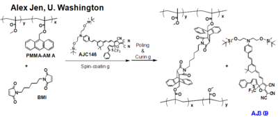
More sophisticated materials are designed to have cross linking groups. Simultaneous poling and crosslinking requires increased attention to process details and control over process variables.
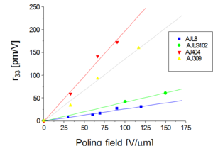
EO polymer evolution - r33
In the last few years there has been a significant improvement in thin film poling. A larger field results in a higher R33, unfortunately there is dielectric breakdown at higher field strengths.
The high R33 materials have increasing absorption in the infrared range. The infrared tail is in 700 – 800 nm.
Theory of multilayer poling
To pole a polymer on cladding you have to know the temperature dependent and time dependent electrical conductivity of all the materials as function of time.
For the EO polymer
- <math>j = \frac {4 \pi em (kT)^2} {h^3} exp \left (- \frac {\phi - \beta_s \sqrt{E}} {kT} \right )\,\!</math>
For the Sol-gel Cladding
- <math>j= \frac {9} 8 \epsilon \mu_n \frac {V^2} {d^3}\,\!</math>
See Sprave 1998 [1] See Blum 1998 [2]
Typical poling profile
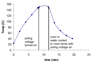
We did numerous experiments to come up with a an optimal poling technique. For example first heat the sample to 140 °C, turn on the poling voltage at 7 minutes, for 3-4 minutes, then cool it off with active cooling
It is possible to get better poling with a the sol-gel cladding present because it was possible to increasing the poling voltage without having dielectric breakdown. Normally researchers struggle to get EO performance to be maintained after adding cladding.
Modulators
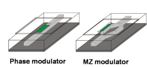
A phase modulator has a single waveguide which passes through a EO material. When the material is energized it changes the index of refraction and slightly changes the phase of the light passing through. To make use of this behavior you have to have a lot of surrounding electronics.
The drive voltage for a simple phase modulator Vpi(PM) is given by
- <math>V\pi(PM)= \frac {\lambda} {r_{33}(n^{TM})^3 - r_{13}(n^{TE})^3} \frac {d} {L \Gamma}\,\!</math>
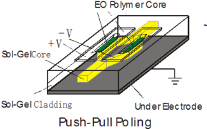
A Mach Zehnder device is more complicated but easier to use. Light can be turned on and off by interference controlled by the applied voltage. If the EO material is applied to both side it allows for push-pull poling which can be used to completely reverse the current. This allows you to reduce the drive voltage by a factor of 3.
The drive voltage for a Mach Zehnder modulator is given by :(assuming r33~r13)
- <math>V_\pi (MZ) = \frac {\lambda} {r_{33}(n^TM)^3} \frac {d}{ L \Gamma}\,\!</math>
- <math>\Rightarrow V_\pi (MZ) = V_\pi(PM) / 1.5\,\!</math>
The drive voltage for push pull poling is given by
- <math>V_\pi(PP) = V_\pi (MZ)/2 = V_\pi (PM)/3\,\!</math>
see more on Mach Zehnder devices Second-order_Processes#Technological_Applications_Of_The_Pockels_Effect
AJ309 phase modulator
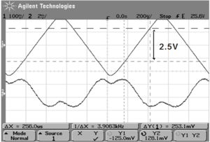
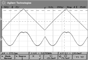
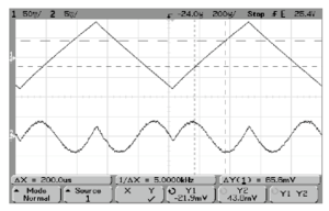
Using AJ309form Alex Jen in a phase modulator we can calculate the drive voltage Vpi., that is the voltage difference it take to go from extremes in the produced wave. This can be worked backwards to arrive at an R33 of 170 pm /V
| EO Polymer | Vπ(electrode) | r33@ λ= 1550 nm |
|---|---|---|
| AJLS102 | 7.6V (2.4 cm) | 56pm ?V (d=15μm) |
| AJ309 | 2.5 (2.4cm) | 10 pm/V (d = 15& mu;m |
See Enami 2007 [3]
Index Tapering
Novel techniques can be used to reduce the thickness of the device in order to reduce the Vπ
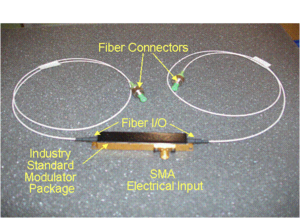
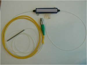
Packaged dual drive MZ modulator
In the finished modulator device electrical contacts are at the side while the input and output light access either end.
- Angle cut input and output facets
- Glass/high index epoxy (>100micron) CYTOP(1.8 micron) on passive regions
- Polarization is not controlled (non PM fiber)
- Vπ = 3.6V for 2.4cm electrode
All Optical Switching and All Optical Signal Processing
All optical switching (AOS) uses an input light of one wavelength to control the passage of light of another wavelength, analogous to how the gate voltage of a transistor opens and closes a circuit. All optical signal processing (AOSP) extends this to modulate a signal frequency again using light rather than an electrical signal as the gate.
Unlike silicon nitride waveguides where evanescent coupling occurs above the guide, silicon-based devices still possess the unique ability to provide extremely strong confinement of the evanescently coupled wave inside a nano-slotted waveguide. This provides sizable intensities which, when coupled with the large nonlinearity of the chromophore, permits the use of reduced interaction lengths allowing for smaller devices and the potential for chip-scale integration. For this reason, organic-silicon based photonics still remain a critical area of interest for AOSP.
Conclusion
Properly engineered optical polymers present both performance and cost advantages when compared to their inorganic counterparts.
The factors leading to optical loss in passive optical polymers are now well understood, and several systems competitive with silica-on-silicon have been demonstrated and commercialized (Dupont Photonics, Asahi Glass, Photon-X) for filter and thermo-optic devices
Recent advances in EO polymers enable higher performance devices (~0.5 V) as well as fundamentally new device designs
The fundamental connection between macroscopic activity (r33) and loss needs to be further understood. If we could get to a loss that was as good as passive polymers were to begin with.
Waveguide cladding layers are critically important in EO modulators, as they must be good conductors during poling and good dielectrics during operation, with low optical loss and, ideally, tunable refractive indices and easy patternability.
Thermal and photo stability are issues. EO activity will decay under normal operating temperatures that are close to the glass transition temperature. Infrared light can be absorbed by oxygen to become an aggressive radical species which is able to attack the chromophores. This can be solved by proper packaging. Thermal stability remains an issue.
References
| Previous Topic | Return to Organic Photonics Applications Menu | Next Topic |
